When it comes to the word “yield,” there are many different meanings. For a chip foundry, yield means the percentage of usable chips diced from a silicon wafer that passes quality control. If a foundry has a low yield, it makes the chip cost more expensive since a larger number of wafers are required to manufacture the number of chips needed. That results in lower profit margins, and possible supply shortages.
To understand why the process node is so important just keep one simple thing in mind: as process numbers go lower, transistor sizes typically get smaller. This increases the transistor count and the transistor density of the chip. The former is the raw number of transistors shoehorned into a chip while the latter is the number of transistors squeezed into a specific area of the chip. Higher numbers for both usually result in a component that is more powerful and/or energy efficient. So as process number shrink, performance and efficiency increase.
TSMC’s 2nm node includes a new transistor called Gate-All-Around (GAA). Using vertically positioned horizontal nanosheets, GAA transistors surround the channel on all four sides. The previous generation of transistors, known as FinFET, only covered the channel on three sides. GAA transistors have less leakage and higher drive currents resulting in improved performance.

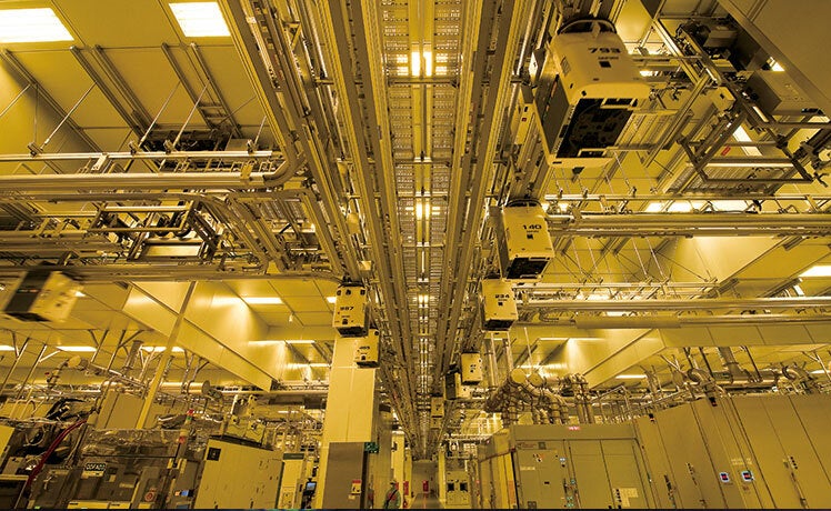
Inside of a TSMC fab in Taiwan. | Image credit-TSMC
