TECHNOLOGY

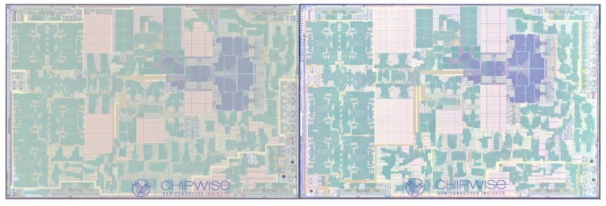
Die shots of the new A18 and A18 APs prove that Apple has designed two different chipsets

×

Die shots of the new A18 and A18 APs prove that Apple has designed two different chipsets

Share this article
Die shots of the new A18 and A18 APs prove that Apple has designed two different chipsets


Apple powers the non-Pro iPhone 16 models with the A18 application processor (AP) while the iPhone 16 Pro and iPhone 16 Pro Max are equipped with the A18 Pro AP. Both are manufactured by TSMC using the Taiwan foundry’s second-generation 3nm process node (N3E). The only difference between the two chipsets based on the information released by Apple is that the A18’s GPU has five active cores compared to six active cores for the GPU on the A18 Pro. 

Considering that Apple released limited information about the new SoCs, there was speculation that the tech giant was engaging in a process called chip binning. The latter process would use A18 Pro chips made with a GPU core that didn’t meet Quality Control. With five good GPU cores, the defective A18 Pro AP would be repackaged as an A18 AP for the iPhone 16 or iPhone 16 Plus. Both APs have six CPU cores (made up of two performance cores and four efficiency cores), and Apple didn’t reveal how many transistors each AP is packed with.

But die shots of both chips reveal that the A18 Pro carries many more transistors than the A18 which means that Apple is not using chip binning and has designed two separate chips. If Apple was using chip binning, both the A18 and A18 Pro would have the same number of transistors which they don’t. This also means that the A18 Pro is more powerful and efficient than the A18. The transistors show up in the die shots as lighter areas.

Still, there are some similarities as both chipsets will support Apple Intelligence and include hardware-based ray tracing. The latter delivers more realistic lighting in a video game scene including light reflections, refractions, shadows, and more. This year’s A18 and A18 Pro continue to use TSMC’s InFO-PoP (Integrated Fan-Out Package-on-Package) method. This allows the DRAM package to be placed on top of the SoC die instead of including it in a separate die.
While there had been early speculation that Apple would debut TSMC’s new 2nm process node with the A19 Pro chip expected to power the iPhone 17 Pro and iPhone 17 Pro Max next year, the latest word from TF International analyst Ming-Chi Kuo is that Apple will have the A19 and A19 Pro chipsets manufactured next year by TSMC using the foundry’s third-generation 3nm node (N3P). That would result in the debut of TSMC’s 2nm node with the A20 Pro AP expected to power the iPhone 18 Pro and iPhone 18 Pro Max in 2026.

When TSMC switches over to 2nm production for Apple’s A20 Pro AP, it will be the first time the chipset running the iPhone will use Gate-All-Around transistors. With these transistors, the gate comes into contact with the channel on all sides reducing current leaks and improving the drive current.


Source Link Website

Leave a Reply

Your email address will not be published. Required fields are marked *